 Non-Destructive Testing Non-destructive testing (NDT) refers to a wide group of analysis techniques used in science and industry to evaluate the properties of a material, component or system without causing damage. As the name suggests, it means testing things without destroying them so that the component can still be used after the test. By doing so, NDT methods allow manufacturers to inspect components and assess flaws, and ensure products and infrastructure meet safety and quality standards.
Visual Testing One of the simplest and most common Non-Destructive Testing techniques is visual testing. It involves close visual examinations of parts or structures, typically augmented using aids like mirrors, magnifiers or borescopes. Visual inspections allow the detection of surface defects, material abnormalities or degradation. While basic, it remains a valuable testing method due to its low cost and ability to find issues without needing specialized equipment. Visual testing is commonly used in applications like pre-delivery vehicle inspections. Magnetic Particle Testing Magnetic particle testing utilizes magnetic fields to detect surface and shallow subsurface flaws in ferromagnetic components and materials. The part is magnetized, usually by passing an electrical current. Iron or aluminium oxide particles are then applied which will be attracted to any discontinuities or imperfections in the material. The particles cluster at crack or defect locations making them visible to the inspectors. It is very effective at finding cracks or lack of fusion in ferrous metals and alloys. Applications range from railway wheels and pressurized vessels to jet engine components and welded structures. Liquid Penetrant Testing Liquid penetrant testing utilizes a penetrant fluid which flows into surface-breaking defects when applied to the test part. After allowing time for capillary action to draw the penetrant into any cracks or flaws, excess penetrant is removed before a developer is applied. The developer draws the penetrant out of defects and makes them visible, usually appearing as a red color against the white background. It is effective on both ferrous and non-ferrous materials, though lacks the sensitivity of magnetic particle testing for some applications. Liquid penetrant testing is commonly used in general manufacturing, aerospace, and automotive industries. Radiographic Testing Radiographic testing employs either X-rays or gamma rays to non-destructively view the internal structure and discontinuities of an object. X-rays are generated externally and passed through the part to expose a photographic film on the other side. Any defects causing attenuation of the beam will appear on the processed film. Alternatively, radiotracers can be introduced in liquids where gamma photons interact with matter to expose film within the part. Radiography provides interior views not possible with other methods, allowing detection of defects like cracks, porosity, corrosion or foreign objects with high sensitivity. It sees widespread use in applications like aircraft, pressure vessels, pipelines, castings and welds. Ultrasonic Testing Ultrasonic testing works on the principle of high-frequency sound wave propagation and interaction. A transducer transmits pulsed ultrasonic waves into the test object which then reflect back to the transducer from any internal flaws or imperfections they encounter. Characteristics of the reflected ultrasound provides information about defect size, orientation and location which is displayed using instruments like A-scans and frequency analysis. Coupling media like water is often used to efficiently transmit ultrasound into the part material. With advanced techniques like phased arrays, ultrasonic inspection is able to detect both surface and subsurface defects to significant depths in metals, composites and castings. Eddy Current Testing Eddy current testing exploits the principles of electromagnetic induction to detect flaws. A high-frequency alternating current is passed through a coil probe which induces circulating eddy currents within a conductive part. Any discontinuities or changes in part thickness cause a perturbation in the eddy currents which is measured by the probe coil. This allows detection of fatigue cracks, corrosion, metallic coatings and other surface or near surface issues without direct contact. Handheld eddy current equipment is flexible for use on complex parts and structures like aircraft components where other methods may be difficult. It offers high sensitivity to changes at or just below the surface. Acoustic Emission Testing When defects grow or materials undergo plastic deformation, small stress waves are emitted known as acoustic emissions. By monitoring these unique sound waves, acoustic emission testing can identify the movement and acceleration of flaws in real-time. Sensors are attached to a structure to continuously listen for transient elastic waves produced during defect growth or crack formation. Pattern recognition software then analyzes the resulting acoustic signatures to characterize sources for structural health monitoring applications. The technology has growing usage in monitoring pressure vessels, rotating equipment and composite structures due to its passive nature requiring no external stimulus. Advancing Non-Destructive Testing These established NDT techniques continue advancing through improvements in equipment, capabilities and data analysis methods. New techniques also emerge addressing gaps not well served by existing options. For example, digital radiography now offers faster inspection times and detectors with improved sensitivity. Thermography uses infrared cameras to detect subsurface flaws by interpreting heat patterns. Guided-wave ultrasonics is capable of scanning large areas by transmitting Lamb waves along structural surfaces. Emerging applications of non-destructive testing ensure safe and cost-effective quality control across industries by providing a crucial layer of inspection without compromising product or system integrity. Proper material verification enables critical infrastructure to reliably operate well into the future. Get More Insights On Non-Destructive Testing
0 Comments
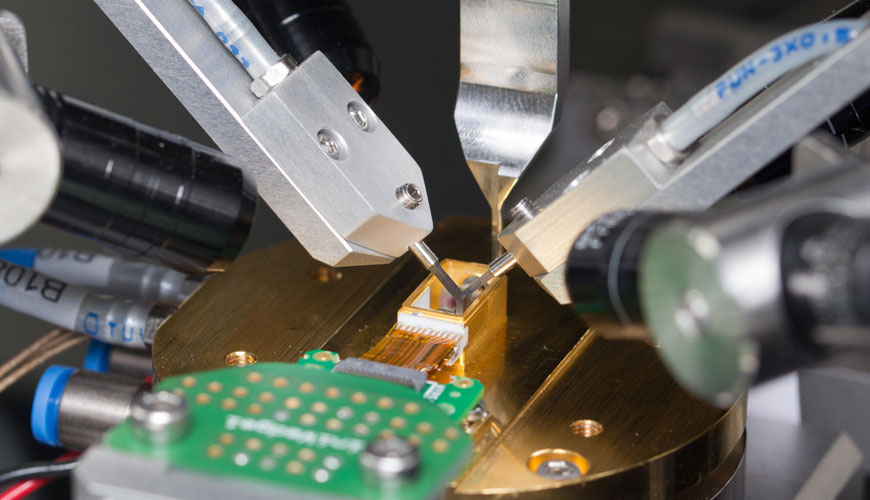 Silicon Photonics Silicon photonics refers to the manipulation of light or photons on a silicon chip. Just like electronic chips facilitate transmission and processing of electronic signals between different components; photonic chips can guide and control light on a small scale utilizing semiconductor materials. Silicon is an ideal medium for integrated photonic circuits due to its transparency to near-infrared light and its compatibility with semiconductor fabrication processes.
Understanding Silicon Photonics At its core, Silicon Photonics involves the manipulation of photons, the fundamental particles of light, within silicon-based structures. Unlike conventional electronic circuits that transmit data using electrons, silicon photonics harnesses the speed and bandwidth of light to facilitate rapid data transfer. By leveraging existing silicon manufacturing processes, this technology offers a cost-effective solution for integrating optical functionalities onto silicon chips, enabling seamless compatibility with existing electronic systems. The Promise of High-Speed Communication One of the most compelling advantages of silicon photonics lies in its ability to transmit data at incredibly high speeds over long distances with minimal signal degradation. Traditional copper-based interconnects struggle to keep pace with the ever-increasing demand for bandwidth, leading to bottlenecks and latency issues in communication networks. In contrast, silicon photonics enables the transmission of vast amounts of data at speeds approaching the limits imposed by the laws of physics, thereby unlocking new possibilities for real-time communication and information exchange. Revolutionizing Data Centers Where the processing and storage of massive volumes of data are paramount, silicon photonics offers a game-changing solution for overcoming bandwidth limitations and improving overall efficiency. By incorporating optical interconnects at the chip level, data centers can achieve unprecedented levels of performance and scalability, leading to faster data processing, reduced latency, and lower power consumption. Furthermore, the compact nature of silicon photonics allows for greater integration density, enabling data centers to maximize their computing power within limited physical space. Enabling Next-Generation Technologies Beyond traditional communication networks and data centers, silicon photonics holds immense potential for driving innovation across various fields. From augmented reality and autonomous vehicles to telemedicine and quantum computing, the integration of photonics into silicon-based platforms opens doors to a myriad of applications that were once deemed impractical or unattainable. By seamlessly integrating optical functionalities with existing electronic systems, silicon photonics lays the foundation for a future where communication is faster, more reliable, and more pervasive than ever before. Silicon photonics represents a paradigm shift in the field of communication technology, offering unparalleled speed, efficiency, and scalability for the transmission of data. By harnessing the power of light and integrating it into silicon-based platforms, this transformative technology is paving the way for a new era of communication where the boundaries of possibility are continually being pushed. As we stand on the cusp of this technological revolution, the potential applications of silicon photonics are limited only by our imagination, promising a future where connectivity knows no bounds. Get More Insights On Silicon Photonics 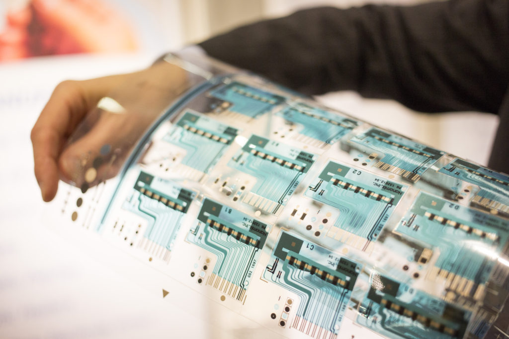 Printed Electronics Printed Electronics
Printed electronics is a new and innovative technology that uses different printing techniques like inkjet printing, gravure printing, screen printing and others to print electronic devices on various substrates like paper, plastic, fabric and more. Some of the key advantages of printed electronics include low-cost manufacturing, versatility in substrates, compatibility with high-volume printing methods and environmental friendliness. Applications of Printed Electronics Displays One of the major applications of Printed Electronics is in displays. Technologies like organic light-emitting diode or OLED displays use printing methods to deposit thin films of organic semiconductors that emit light when electric current is applied. This makes it possible to print large, flexible displays that can be integrated into clothing, smartphones, tablets and more. OLED displays offer better image quality, lower power consumption and more design flexibility compared to LCD displays. Sensors Printed sensors find applications in many areas like healthcare, industrial monitoring, smart packaging and more. Examples include printed gas sensors to detect volatile organic compounds, humidity sensors, strain and pressure sensors, touch sensors and biosensors that can detect biomarkers in fluids. The key advantages are low-cost mass production as well as compatibility with rigid and flexible form factors. Photovoltaics Solar panels are another major application that widely uses printed electronics manufacturing methods. Technologies like organic photovoltaics or OPVs and dye-sensitized solar cells use printing to deposit active layers that absorb sunlight to generate electricity. This makes it possible to integrate solar cells onto buildings, vehicles, wearables and other non-traditional form factors in a low-cost manner. Emerging technologies like perovskite solar cells also rely on printing processes. RFID Tags Radio frequency identification or RFID tags are widely employed for logistics tracking, access control and other industrial applications. Printing methods are used to deposit conductive inks or pastes that form the antennae of RFID tags directly onto substrates. This enables ultra-low-cost production of passive RFID tags for one-time use in packaging and other disposable applications. Embedding RFID tags into printed packaging opens up new possibilities. Advantages of Printed Electronics Manufacturing Some of the key advantages of printed electronics manufacturing compared to traditional silicon wafer processing include: Lower manufacturing costs - Printing techniques can offer extremely high-volume and low-cost production compared to vacuum deposition or etching methods used in silicon chip making. This makes printed electronics suitable for disposable and high-volume consumer applications. Materials versatility - A wide range of substrates like paper, plastic films, glass, fabrics and more can serve as the base for printed electronic components. This results in flexibility in form factors. Scalability - Traditional chip manufacturing requires large investments and has issues with scalability. However, the printing infrastructure in the graphic arts industry provides a readily scalable platform for printed electronics manufacturing. Environmental friendliness - Printing uses less hazardous chemicals and creates less electronic waste compared to chip processing. It also enables recovery and reuse of unused printing substrates. Compatibility with roll-to-roll production - Large area components can be produced continuously and rapidly through roll-to-roll or web processing machinery without the need for maintenance-intensive wet benches or vacuum systems. Challenges and the Road Ahead While printed electronics holds immense promise, several technological and manufacturing challenges need to be addressed for its widespread commercialization: - Printed components still lag behind silicon chips in performance metrics like switching speeds, resolution and lifetime. More research is needed in functional materials as well as multi-layer printing and interconnection techniques. - Precise, high-resolution printing of nano-scale features remains difficult with existing graphic arts machinery. Hybrid printing approaches need to emerge. - Long-term durability and reliability of printed electronics under different environmental conditions requires further testing and improvements through encapsulation and other strategies. - Large-area, high-throughput printing of complex multilayer circuits with different materials remains a bottleneck, limiting true system-level integration. Automation and quality control need advancements. - Commercialization of printed electronics requires long-term partnerships between technical startups, OEMs and printing industries to develop applications, design infrastructure and drive volume adoption. With continued developments, printed electronics is expected to transform manufacturing across sectors by enabling new form factors, services and business models through low-cost production of electronic features directly onto various substrates. Combined with advances in functional materials, interconnection and resolution technologies, this disruptive technology holds the potential for ubiquitous integration of electronics into everyday objects. Increased R&D collaborations and the development of scalable manufacturing infrastructure are key milestones that will drive its global transition from labs to mainstream consumer applications over the next decade. Get more insights, On Printed Electronics |
